1. Handling notes for Crystal Units
I. When dropped by mistake: < All products >
Crystal units are designed and manufactured to resist physical shocks.However, in the event crystal units are subjected to excessive impact such as being dropped onto the floor or subjected to shock during mounting, you will need to make sure its satisfactory performance before using it.
II. Soldering:< Through hole type >
- Lead wires should be soldered within 3 seconds, with the soldering iron heated to a temperature no higher than 380ºC.
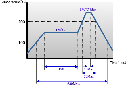
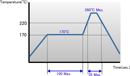
- For solder-dip mounting, it should be within 10 seconds with a temperature no higher than 260ºC. And take care not to heat the whole crystal units in the dip mounting process.Mounting upright is recommended (preventing heat conduction directly to the body of the crystal units).
- Heating the whole crystal units, for example, in a reflow oven may impair their performance. This is because the holder is quite small and it is sealed by press sealing with solder material, so the reflow process is not permissible.
< SMD type products >
- Pb solder
- Pb free solder (excepting CM309E)
- Pb free solder (CM309E)
III. Bending Lead:< Cylinder type products >
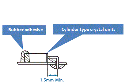
- When the lead of a cylinder type crystal units needs to be bent, leave more than 1.5 mm (3.0 mm is recommended) of lead from the case in order to prevent any cracks of the hermetic seal glass at the root of the lead, and use a jig for bending if possible. Please avoid bending it directly from the lead wire root.
- When bending the lead of cylinder type crystal units, do not scrape off the solder plating from the lead surface.
IV. Mounting:< Cylinder type products >
- Soldering on the body of cylinder type crystal units must be strictly avoided due to deteriorate the characteristics or damage the product. Rubber adhesive is recommended.
-
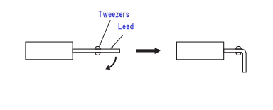
When the lead needs to be bent by hand, follow the instructions below.
– Hold the body of cylinder type crystal units by hand.
– Grip the part that you intend to bend with tweezers. The part where you bend should be more than 1.5 mm from the body case, but we on the part of the hermetic seal glass.
– Press and bend the lead 90 °with the tweezers without pulling the lead strongly. Please be sure that pulling the lead strongly may crack the hermetic seal glass at the root of the lead and may cause the airtightness and the characteristics to deteriorate.
< SMD type products >
When using an automatic loading mounter, test and confirm that no damage has been caused to the characteristics of crystal units before mounting.Bending a circuit board in the process of cleaving boards after mounting and soldering crystal units may cause peeling off the soldering or package cracks by mechanical stress. Please be sure that the layout of the crystal unit position is on the less stressed and the cleaving process is under less stressed for the crystal units.
V. <Cleaning:All products>
- Crystal units may be affected and, at worst, destroyed by ultrasonic cleaning. Please be sure to check if your cleaning process causes any damages to crystal units prior to use.
- Some cleaning fluids may cause damage to crystal units. Please be sure to check the suitability of the cleaning fluid in advance.
2. Handling notes for Crystal Oscillators
I. When dropped by mistake:
Please refer to 1. Handling notes for Crystal Units.
II. Soldering:
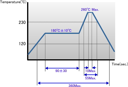
Should be soldered within 10 seconds at no higher than 260ºC or 3 seconds at no higher than 380ºC. Please refer to <SMD type products> in “1. Handling notes for Crystal Units” regarding the reflow profile.
III. Cleaning:
- Crystal oscillators may be affected and, at worst, destroyed by ultrasonic cleaning. Please be sure to check if your cleaning process causes any damages to crystal oscillators prior to use.
- Some cleaning fluids may cause damage to crystal oscillators. Please be sure to check the suitability of the cleaning fluid in advance.
IV. Mounting:
Mounting crystal oscillators reversed may cause malfunctions or damage, so please check the orientation before mounting. When using an automatic loading mounter, please select a machine with low impact and check for damages on the products.
V. Thermal shock:
Repetitive rapid temperature changes with a large amplitude may cause deterioration of the crystal oscillators and break the wires inside the package. Such conditions must be avoided.
VI. Static electricity:
Excessive levels of electricity may cause damage to the IC inside crystal oscillators even if an anti-static electricity protection circuit is provided in the circuit board. Please be sure to use conductive packing materials and transport containers, use a soldering iron and measuring circuit free from high-voltage leakage, and provide a grounding connection while using crystal oscillators.
VII. Noise:
Applying excessive levels of extraneous noise to the power supply or input pin may cause latch-up or spurious phenomena, which results in malfunction and breakdown.Do not permit any object that emits a high level of noise in the vicinity of crystal oscillators.
VIII. Power supply lines:
Line impedance of the power supply should be as low as possible. To maintain stable operation, power supplies to crystal oscillators should have by-pass capacitor (0.01μF ~ 0.1μF). Place the capacitor as close as possible to crystal oscillators supply pins (the VDD pin and the GND pin). The supply lines (the VDD and the GND) should be as thick and short as possible.
IX. Output line:
To reduce the line impedance of the output line and reduce the electromagnetic radiation, the output load should be installed as close as possible to the crystal oscillators.
X. Input line:
The input pin (OE) is pulled up with an internal resister, it should be used at low impedance for noise suppression, but if it is not used, connect it to VDD.
3. Handling notes common to All Products
I. Storage:
Storage of crystal products under higher temperature or high humidity may affect frequency stability or solderability.Please store crystal products under normal temperature and humidity without exposing to direct sunlight or dew condensation, and avoid storing crystal products over the long term: mount them as soon as possible after unpacking.
Handling Notes
Handling notes in Oscillation Circuit Design
To fully utilize the characteristics of crystal units, it is necessary to design an oscillation circuit constant with optimal conditions.
Based on the experience we have accumulated over the years, Citizen Finedevice offers services such as checking the oscillation circuit designed by a customer with regard to points mentioned below to ensure optimal matching between the crystal units and the oscillation circuit. The purpose of this investigation is that we make our products to ensure more safety and ease of use for the customers.
1. MOS crystal oscillation circuit
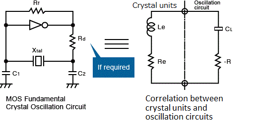
CMOS crystal oscillation circuit
| CL | Load capacitance |
|---|---|
| -R | Negative resistance |
| Le | Effective Inductance |
| Re | Effective resistance |
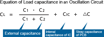
2. Load capacitance (CL)
The load capacitance (CL) refers to the effective external series capacitance in an oscillation circuit assumed to be viewed from the crystal units side. The resonance frequency will be determined based on the load capacitance and the crystal unit. For this reason, differences in the load capacitance of the oscillation circuit may cause frequency deviations (result in a different resonance frequency from the one required).
3. Negative resistance (-R)
The negative resistance reflects the allowance and margin for oscillation motility.An insufficient negative resistance may cause unexpected trouble such as No-Oscillation or slow start-up time.
4. Drive current (i)
The drive current refers to the current flows through crystal units. An excessive drive current being applied to crystal units may cause the following trouble/phenomena.
- Increase in the electromagnetic wave noise
- Crystal unit element of T/F breaking off
- Abnormalities occur in the frequency tolerance over operating temperature range.
- Changes in the characteristics of crystal units
(Changes in the frequency, changes in the motional resistance, etc.)
5. Frequency-voltage coefficient
Represents the rate of frequency change against variations in the supply voltage.The cause of frequency changes due to power supply variation can be attributed more to factors on the oscillation circuit side (especially the IC) than crystal unit s side. It is normally desirable to keep within ±5 ppm in the rate of frequency change against a ±10% variation in the supply voltage.
6. Frequency -Frequency tolerance over operating temperature range
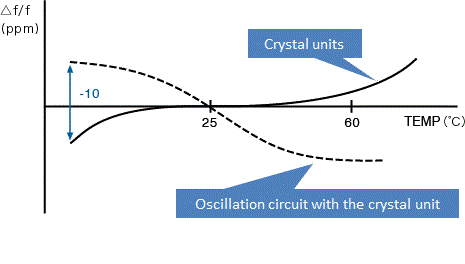
Represents the rate of frequency change against variations in operating temperature.There may be a large difference between the oscillation circuit and the crystal unit in terms of frequency tolerance over operating temperature range.
(Example)Frequency -Frequency tolerance over operating temperature range
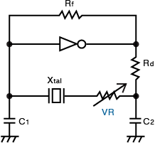
7. How to check the margin for oscillation motility
- To determine the margin for oscillation motility, you should check the negative resistance (-R) of the oscillation circuit.
- Connect a variable resistor (VR) to the oscillation circuit in series with crystal units.Adjust the resistance value of VR from the “no oscillation” status to oscillation startup.The value shall be a negative resistance (-R) when oscillation starts up.
- Adjust values of C1, C2 and Rd such that the negative resistance is at least 5 times larger than the effective resistance in order to secure enough margins for oscillation motility.Please note that it is recommended that -R should be at least 10 times the effective resistance for equipment required to show high quality and reliability, such as automotive components.