- Contact
- Inquiry form
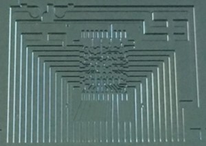
Photolithography
Photolithography is the technology that makes the exposed part and
unexposed part generate characteristic patterns by exposing the
wafer coated with photoresist, a kind of photosensitive material.
Substrate materials include Si, crystal, glass and ceramics.
In addition to photoresist wet films, dry films can also be selected.
Coating methods include film forming, spin coating, electrodeposition and spraying.
Suggestions are provided according to customer requirements.
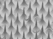
Dry etching
Dry etching is a kind of etching technology utilizing reactive gas.
Deep RIE realizes high-speed machining and high depth-to-width
ratio (opening 1: depth more than 30) based on Bosch process,
and can help penetrate substrates over 2mm.
For products having requirements in verticality, the accuracy level can reach 90.0 ° ± 0.1 °.
In addition to Si etching, parallel-plate RIE provides etching of oxide films and nitride films.
Ion milling realizes etching of various metal films.
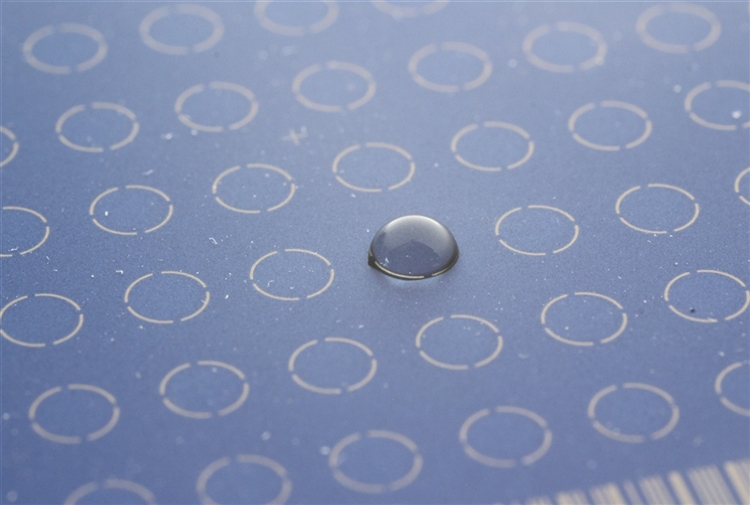
Film forming
From various PVD methods such as sputtering, vacuum deposition, ion plating and thermal oxidation, as well as CVD methods such as TEOS film method, we propose the best scheme for you.
It is possible for the abundant sputtering target materials to realize three-layer overlap in three dimensions simultaneously in the same vacuum.
Metal films, oxide films and polyimide films can be made.
New functions can be added through the combination of thins films.
With hydrophilic, water-repellent and hydrophobic films utilized, the sample control on the cell inspection chips can be realized.
- Contact
- Inquiry form