Technologies available
Lamination Technology
Our lamination process supports both Glass-Silicon and Glass-Glass configurations.
We can use materials that meet your requirements and achieve high-precision lamination.
Regarding silicon substrates, if you provide the wafers, we can handle everything from panel fabrication to module assembly.
Point
- Wafer sizes: compatible with Φ 6, 8, and 12 inch wafers
- Cell Gap: 0.7 μm or more (excellent uniformity and quality)
- Possess high-reliability assembly technology
- If it matches your desired specifications, we can also inject ferroelectric liquid crystal (FLC, our proprietary product).
Know-how
We have a manufacturing system that can handle everything from prototyping to mass production, tailored to your needs.
If you could provide us with your desired specifications,we can propose suitable liquid crystal materials, product shapes, layouts, cell gaps,and other details according to your requirements.
Technology using FLC (Ferroelectric Liquid Crystal)
By utilizing our proprietary FLC, we can develop products with high resolution.
It is also expected that this can be incorporated into products requiring approximately 100 μs high-speed response.*
*However, ON / OFF switching needs to be repeated every 10 seconds.
Leveraging our long-standing expertise, knowledge, and know-how related to FLC, we can propose optimal FLC materials, as well as design and drive conditions for FLC cells.
Point
- High resolution
- High-speed response: approximately 100 μs
- Compatible with visible to near-infrared regions
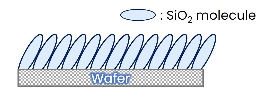
SiO2 deposition technology
SiO2 deposition is a crucial process for controlling the alignment of specific liquid crystal.
Our SiO2 deposition technology enables highly precise control of the molecular orientation of SiO2.
Liquid crystal products manufactured using our SiO2 deposition achieve improved high contrast and light resistance.
|
Detailed diagram of alignment |
Thinning / Miniaturization technology
We have extensive experience in manufacturing ultra-compact and ultra-thin optical elements.
Achievements
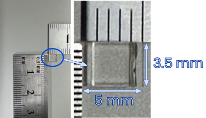
- Ultra-compact optical elements: minimum size of 3.5 mm × 5.0 mm
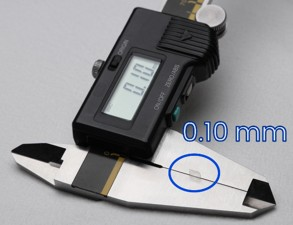
- Ultra-thin optical elements: thickness of 0.10 mm
|
Ultra-compact optical elements |
Ultra-thin optical element |